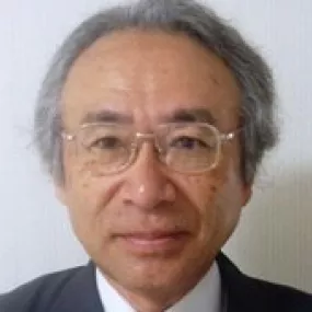
Takeshi Hattori
Owner and Representative Director, Hattori Consulting International (Invited)
Takeshi Hattori, Ph.D. is the Representative Director of Hattori Consulting International. He worked at Sony Corporation in Japan for 36 years, contributing to the development and contamination-control engineering of CCD/CMOS image sensors, Play Station processors, and various other devices.
Since retiring from Sony, he has provided technical consulting services to several Japanese and Korean companies including Tokyo Electron, SEMES, and SK Siltron. He also served as a visiting professor at Hanyang University in Ansan, supervising graduate students' research on wafer cleaning. He is a Fellow of the Electrochemical Society (ECS) and received the Warner Kern Award for his outstanding contributions to the development of innovative wafer cleaning technologies. He has served on the executive/program committees for international symposia such as ECS-SCST, UCPSS, and ISSM. He has authored and edited a book entitled "Ultra Clean Surface Processing of Silicon Wafers -Secrets of VLSI Manufacturing." He can be reached at [email protected].
END