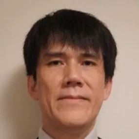
Mitsuhiro Omura (Invited)
Chief Specialist, KIOXIA
Mitsuhiro Omura, Ph.D. joined 3D flash memory development team to create high-aspect-ratio etching processes of stacked films in 2007. He is currently chief specialist of dry etching technology at the Advanced Memory Development Center, Kioxia Corporation, Yokkaichi.
Prior to joining 3D flash memory team, Omura worked on the development of dry etching process for DRAM, Flash memory, high-end CMOS, SRAM, CMOS Sensors especially about dielectric film etching at Process and Manufacturing Engineering Center, Toshiba Corporation, Yokohama.
Omura received his Ph.D. degree in Electronic Engineering from Nagoya University, Nagoya, for his research on plasma etching processes of dielectric materials using capacitively coupled plasmas.