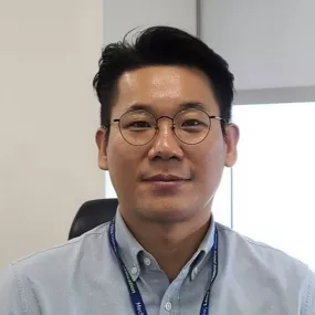
Myungjun Lee
Head of Group, Inspection Solution Group, Mechatronics R&D Center, Samsung Electronics
Myungjun Lee (Ph.D) is the head of inspection solution group in Mechatronics R&D Center at Samsung Electronics, leading to develop the innovated metrology, inspection, characterization solutions for the advanced semiconductor devices since 2017.
Prior to joining Samsung, Dr. Lee was the research scientist of 5D division (lead by Mark D. Smith) at KLA-Tencor in Milpitas, CA, and principal engineer working for Strategic Lithography Team (lead by Harry J. Levinson) at GlobalFoundries, where he was the GF assignee in the pathfinding patterning team at IBM in Albany, NY. His roles were developing advanced patterning (OPC, RET) and process control solutions for the advanced semiconductor devices.
From 2010 to 2011, Dr. Lee was a postdoctoral fellow at University of California at Los-Angeles (UCLA), where he developed the various computational imaging techniques with Prof. Aydogan Ozcan. He received his Ph.D under Prof. Mark A. Neifeld in electrical computer engineering & optical sciences from university of Arizona in 2010, a master degree from Texas A&M University in 2005, and a bachelor degree from Korea University in 2002.
He has authored/co-authored > 40 journal and conference papers, and holds > 30 patents in various optical system designs and algorithms for the applications of imaging, sensing, communications, semiconductor patterning and metrology.