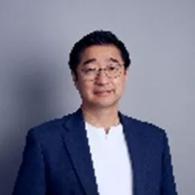
JongWon Shon
VP / Process Technology, ASM
Highlights
- 1993
- Ph.D. received from University of Illinois, Urbana, Champaign
- 1993~1999
- Worked at Lawerence Livermore National Lab and Sandia National Lab as a Staff Scientist. Research Areas include Fluorine plasma etch mechanism, Downstream plasma etching modeling and simulation. Laser fusion simulation using fluid particle simulation.
- 1999~2005
- Worked at Lam Research for Dielectric Etcher development. Run Joint Development Program with Samsung Semiconductors for 5 years.
- 2005~2011
- Worked at Jusung Engineering in Korea for developing HDP CVD, Poly Etcher, PECVD SiN for Solar Application.
- 2011~2014
- Worked at GEN Semiconductor for Vice President developing MRAM Etcher, VHF PECVD, Dry Clean Equipment development.
- 2015~
- Started to work at ASM Korea until today.
Education
- 1985
- Oregon State University, Corvallis, OR BS at EECS, CS and Mathematics
- 1993
- University of Illinois, Urbana, Champaign MS and Ph.D. at EECS
Experience
- 1993 - 1999
- Sandia National Lab, Lawerence Livermore National Lab
- Plasma Etch Chemistry, Modeling, Simulation, Laser Fusion Simulation, Statistical Mechanics
- 1999 - 2005
- Lam Reserch Senior Staff
- Dielectric Etch, Leading JDP with Samsung Semiconductors for 5 years
- 2005 - 201
- JUSUNG ENG, VP
- 2011 - 2014
- GEN VP
- 2015 ~
- ASM Korea VP ,
Other
- As a secretary of GEC(Gaseous Electronics Conference), successfully held 2005 GEC conference at San Francisco. GEC is under American Physical Society and has more than 70 years of history.
- 1992 Elected for President of Korean Student Association at UIUC
- 1999 Secretary of Korean American Scientists in Bay Area
- Publication 24, Patents 2, More than 100 times as a invited speaker.